Surface analysis
The surface of a material often plays a special role for its later use, whether due to protective effects by coatings or modified properties by selected structures.
In addition to high-resolution imaging and chemical analysis of surfaces, we also offer profile imaging to determine layer systems by means of FIB cross-section. In addition to the possibility of tribological and electrical characterization of a surface, we can also selectively change properties using the laser structuring technique xDLIP.
Laserstructuring and tribology
The possible applications of this technique are wide-ranging. An excerpt of them is shown below:
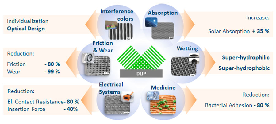
This technology has great potential, for example, in the control of tribological effects. By means of DLIP, a significant reduction of friction and contact areas can be achieved or the service life of lubricating films can be extended manyfold.
The tribological properties can then be assessed on a micro- or nanotribometer. On both devices, we determine friction and wear values of tribologically stressed material pairings.
Further materials engineering development with DLIP takes place at MECS, with future industrializations being carried out by SurFunction GmbH, which was spun off in 2020.
In 2016, the development of the DLIP system was awarded what is probably the most important innovation prize in the field of lasers, and our subsequent successful industrial transfer with TE Connectivity GmbH was awarded the Steinbeis Foundation Transfer Prize in 2019.
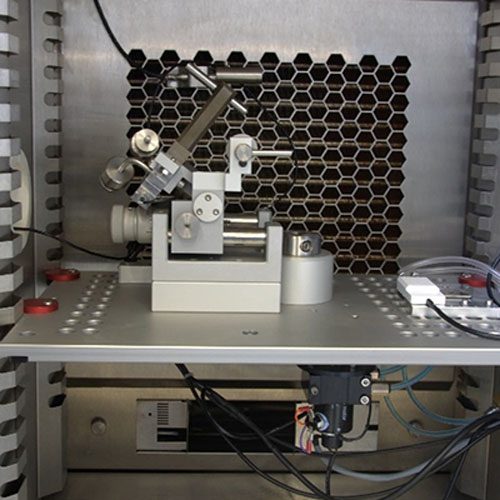
CSM Instruments Mikrotribometer
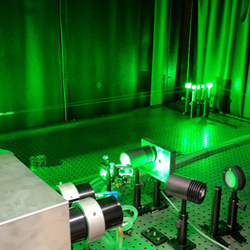
Spectra Physics Nd: YAG ns-Pulslaser
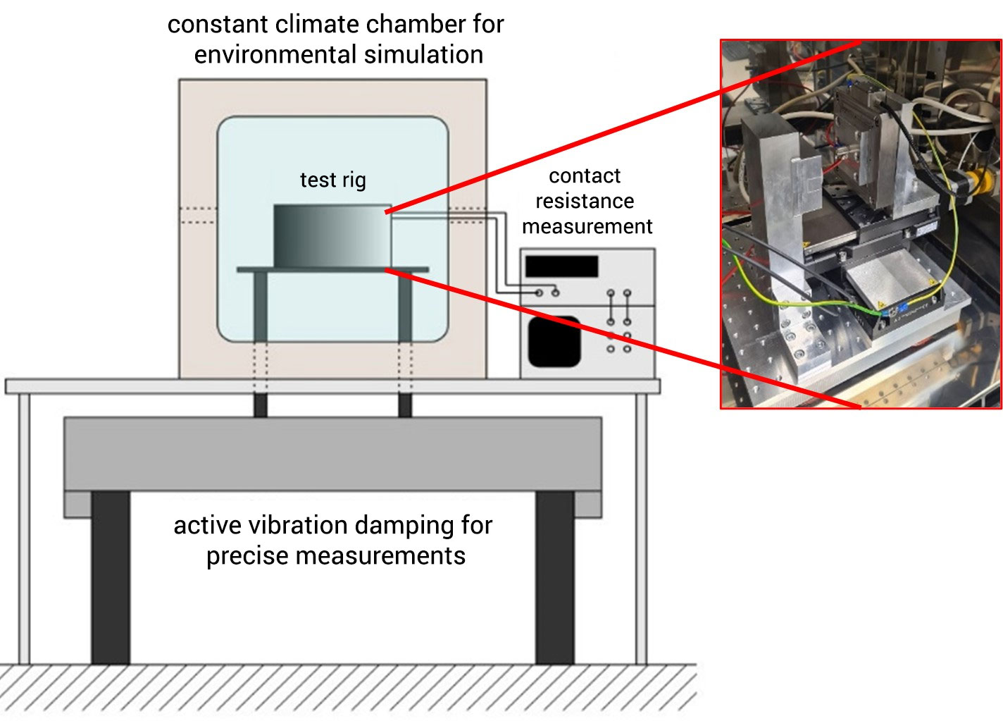
ECR
With the help of various test benches, we can reliably determine electrical contact or transition resistances under variable environmental conditions. This setup is interesting for connectors, for example, as it enables parallel measurement of contact resistance, mating force and coefficient of friction (see Triboelectric Applications).
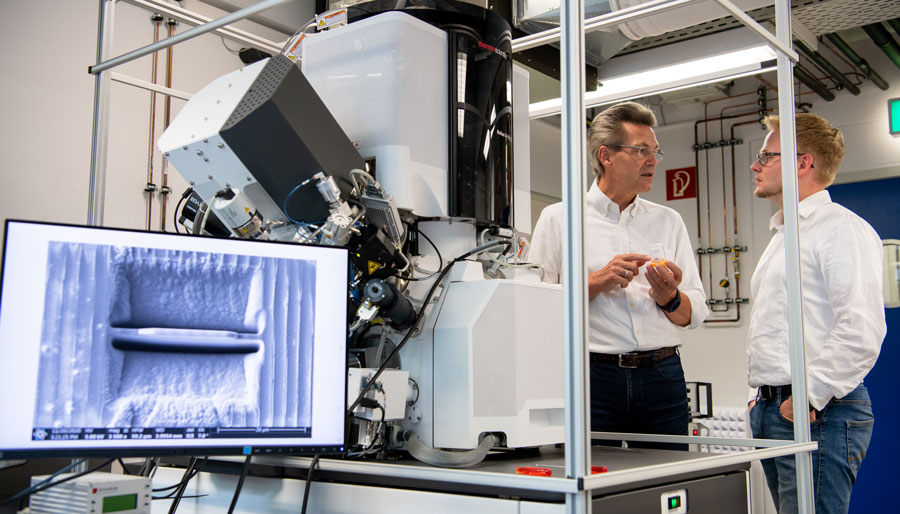
Analysis FIB-REM + EDX/ EBSD
Due to the high resolution down to the sub-nm range, the SEM is our standard tool for the investigation of:
- Precipitates and inclusions
- Layer systems
- Grain sizes
- Pores and other sub-µm structures
The combination of FIB and SEM adds the following capabilities to our repertoire:
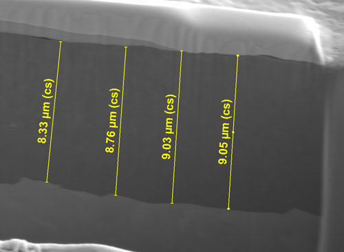
- Generation of near-surface cross sections (view example video)
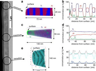
- Characterization of thin films and layer systems
- Preparation of STEM and APT samples
- 3D representation and calculation of microstructures
Additional built-in systems allow us to perform a holistic assessment:
- Chemical analysis of particles, layers or element distributions (EDX)
- Analysis of crystal orientations, grain size distributions, dislocation densities, textures, deformations and preferred directions (EBSD)
- Reconstruction of former austenite grains from EBSD data
- Investigation and chemical analysis of precipitates, phases and layers down to the sub-nm range (STEM incl. STEM-EDX)
- Locally resolved repairs, production of precise mask geometries and special mechanical components, targeted deposition of conductive and non-conductive compounds (micromachining) (view example video)
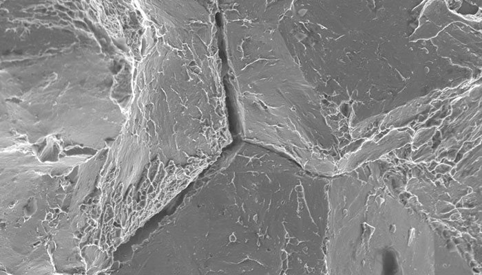
Hydrogen Embrittlement
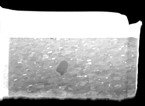
STEM-Analysis
Further examinations
Microscopy
We are able to precisely prepare, contrast and analyze materials. In addition to metallographic preparation options, we have light, laser scanning and scanning electron microscopes at our disposal.
Contact for questions
Dr.-Ing Dominik Britz
Deputy Head MECS Saarbrücken
Adrian Thome, M. Sc
Project Leader
