Material analysis
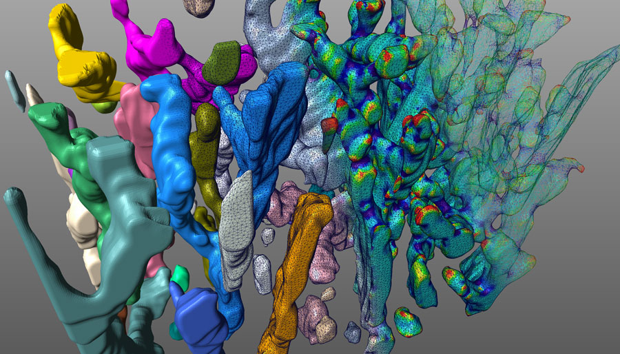
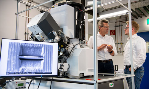
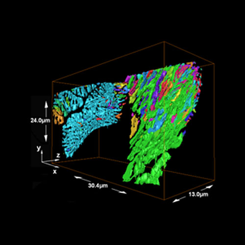
For high-resolution and extremely precise questions in addition to FIB, SEM, EDX and EBSD examinations, we have the capability for 3D tomographies in the micrometer range and atomic probe tomographies in the nanometer range.
Chemical analysis using spark spectrometry
Material analysis plays a decisive role in the quality control of incoming and outgoing goods, process monitoring and also in possible mix-up checks. With the help of our fully equipped spark spectrometer, we can determine the chemical composition of samples down to the lower ppm range within a few minutes.
Complementary examinations for structural analysis, REM-EDX or atom probe tomography are also possible with us.
The maximum equipment of our device allows us to examine alloys based on the following elements:
- Iron including low and high alloy steels and cast iron
- Aluminum
- Copper
- Nickel
- Titanium
- Cobalt
- Tin
- Zinc
- Lead
- Magnesium
X-ray diffraction analysis
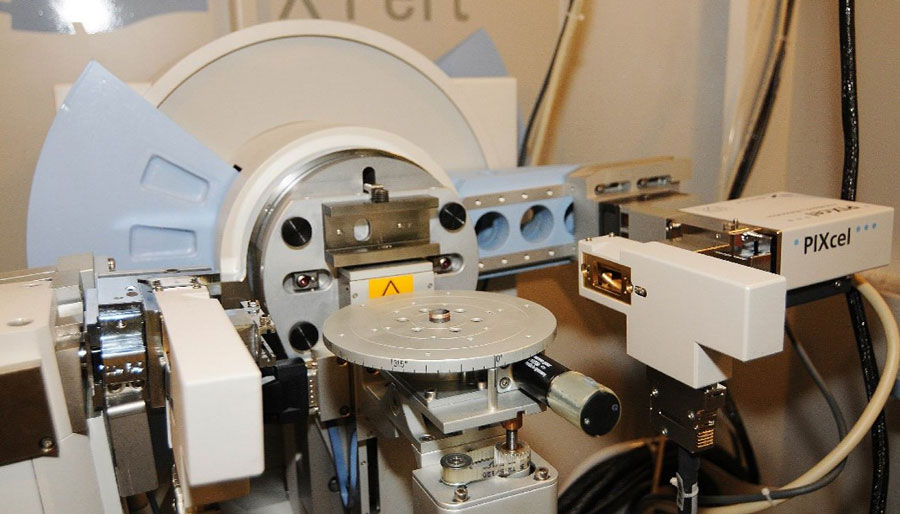
PANalytical Xpert Pro MPD
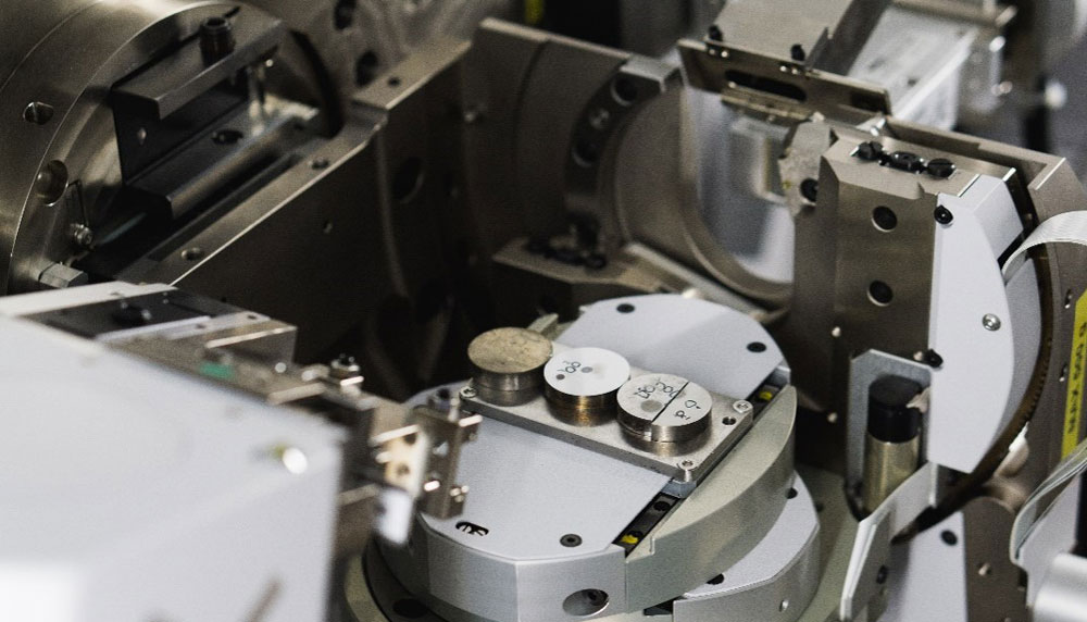
PANalytical Empyrean
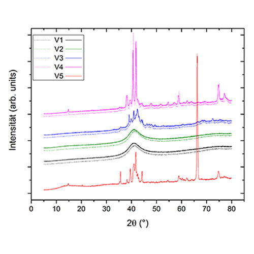
Due to their diversity and precision, integral X-ray diffraction analysis methods are among the most important methods of phase-specific material characterization. With our devices we can determine the following information:
- Qualitative and quantitative determination of phases, their compositions as well as their proportions of the sample volume
- Crystalline structures (e.g. structure, lattice constant, interplanar spacing)
- Presence of amorphous phases
- Lattice defects, density of dislocations, stoichiometry
We can also perform profitable measurements to describe the microstructure state:
- Residual stress analysis to determine the existence and magnitude of manufacturing- or application-related, near-surface residual stresses
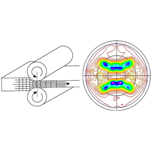
- Texture analysis for detection of preferred orientations of crystallites on surfaces and coatings
Special insertable optics allow us to offer additional measurements:
- Grain size determination of nanocrystalline materials
- Determination of the deformation state, thickness and quality of thin films
- Measurement of single crystals and their perfection
Our built-in high-temperature chamber allows phase analyses under vacuum or inert gas atmosphere at temperatures up to 1200 °C.
Phase analysis as well as stress and texture analysis are possible with suitable sample material down to the micro range with up to 50 µm local resolution.
To achieve an improved signal-to-surface ratio and thus provide more precise results, we can also perform particularly low-surface phase analyses. The combination of these techniques is almost unique for laboratory diffractometers and state-of-the-art in laboratory technology.
Microstructure analysis with REM, FIB and APT
Due to the high resolution down to the sub-nm range, the SEM is our standard tool for the investigation of:
- Precipitates and inclusions
- Layer systems
- Grain sizes
- Pores and other sub-µm structures
The combination of FIB and SEM adds the following capabilities to our repertoire:
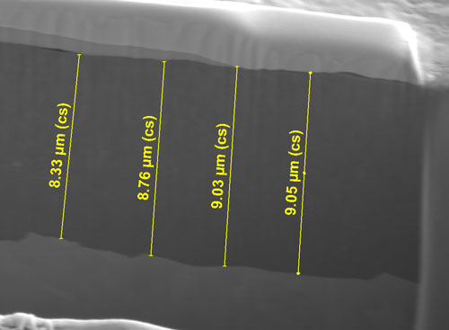
- Generation of near-surface cross sections (view example video)
- Characterization of thin films and layer systems
- Preparation of STEM and APT samples
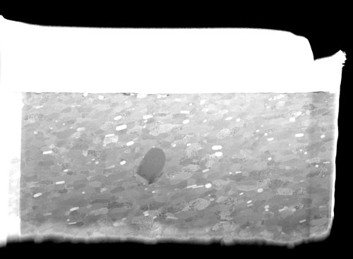
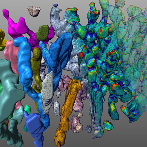
- 3D representation and calculation of microstructures
In the field of damage analysis, we can identify and analyze the following defects with our systems:
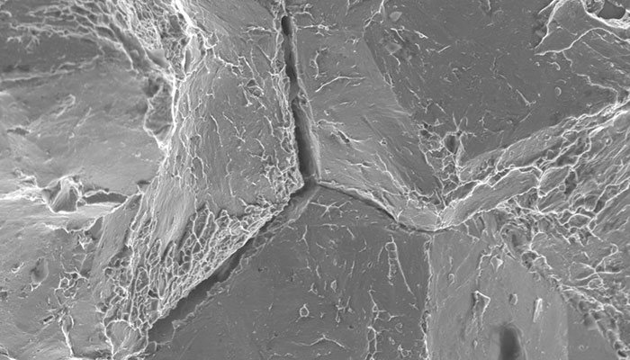
- Fracture surfaces
- Crack propagation and crack evaluation
- Hydrogen embrittlement
- Foreign inclusions
Additional built-in systems allow us to perform a holistic assessment:
- Chemical analysis of particles, layers or element distributions (EDX)
- Analysis of crystal orientations, grain size distributions, dislocation densities, textures, deformations and preferred directions (EBSD)
- Reconstruction of former austenite grains from EBSD data
- Investigation and chemical analysis of precipitates, phases and layers down to the sub-nm range (STEM incl. STEM-EDX)
- Locally resolved repairs, production of precise mask geometries and special mechanical components, targeted deposition of conductive and non-conductive compounds (micromachining) (view example video)
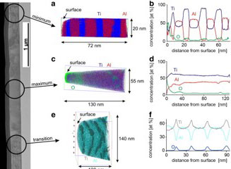
In addition, we can offer three-dimensional material analysis of a wide range of materials on a de facto atomic scale by means of atom probe tomography (APT) in the nanoscale range with analysis sensitivities of up to 5 ppm.
Hydrogen Embrittlement
Analysis 3D-Tomography
Further Examinations
Surface analysis
In addition to the representation and analysis of surfaces, we also offer profile recordings to determine the layer system. We are not only at your side with the surface characterization, but can also change properties in a targeted manner.
Contact for questions

Dr.-Ing Dominik Britz
Deputy Head MECS Saarbrücken

Adrian Thome, M. Sc
Project Leader
