Microscopy

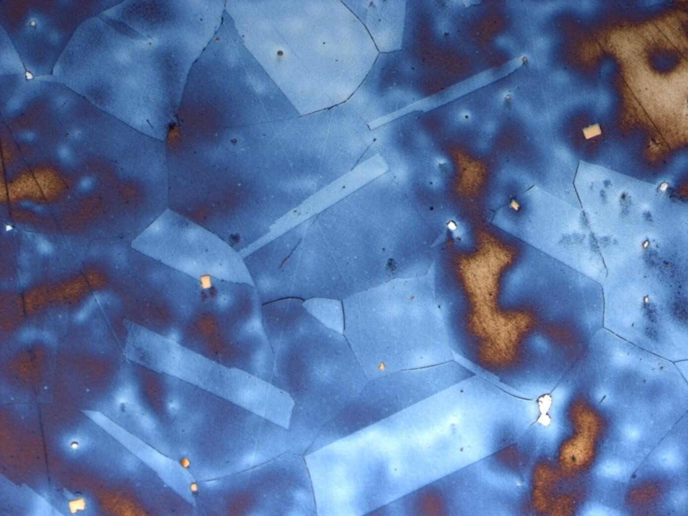
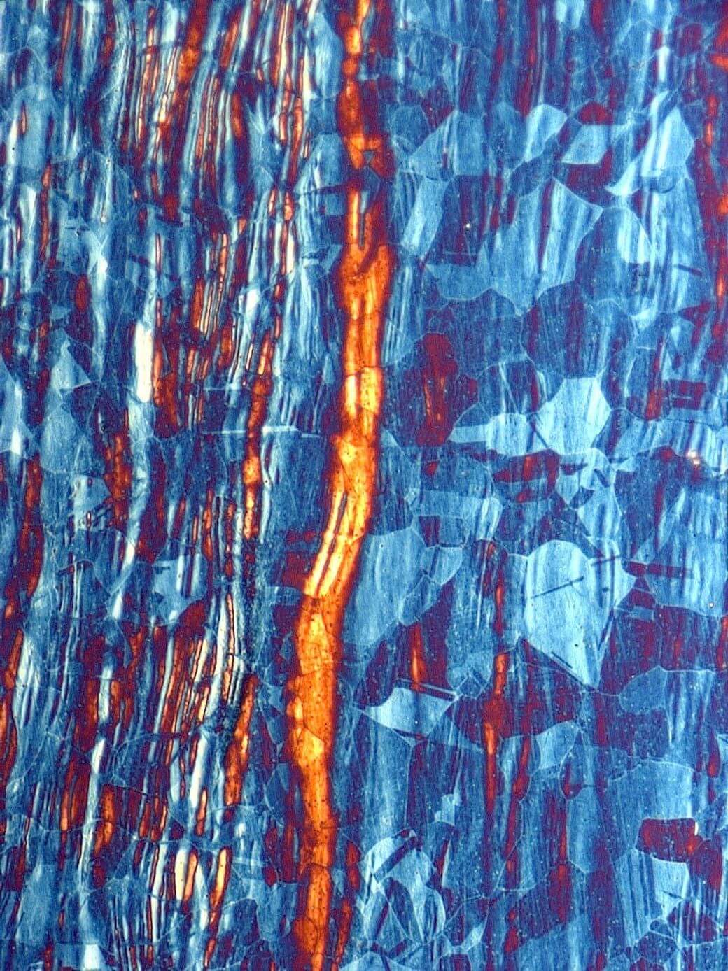
The microstructure knows everything. It stores the previous manufacturing route in its structure and specifies the properties of a component. To gain access to this knowledge, we can prepare, contrast and analyze materials in a wide variety of ways and with great precision. In addition to the entire range of metallographic preparation options, we have light, laser scanning and scanning electron microscopes at our disposal for this purpose.
Materialography
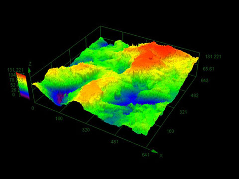
The visualization of the microstructure is then performed with one of our light and laser scanning microscopes. The latter is additionally used for high-precision determination of 3D surface characteristics such as roughness or texture with a height resolution down to 10 nm.

Click on the slideshow to enlarge the images
The following material characterization can be carried out by us:
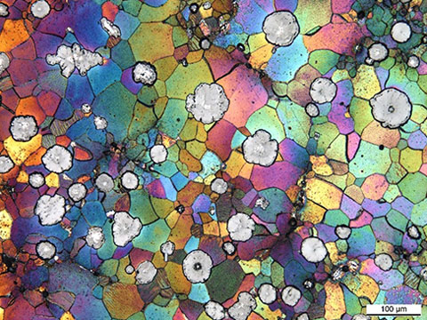
- Microstructure evaluations including control of heat treatments, segregations and precipitations
- Roughness measurements
- Hardness measurements
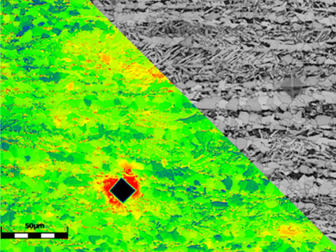
Quantitative microstructure and image analysis can give access to additional information:
- Phase fractions
- Particle sizes and particle proportions
- Grain sizes and grain size distributions
- Layer thicknesses
- Dendrite arm spacings
- Spheroidal graphite analysis
- Lamellar graphite analysis
ThEtching
You can see sample visualizations in the following video clips:

Analysis FIB-REM + EDX/ EBSD
Due to the high resolution down to the sub-nm range, the SEM is our standard tool for the investigation of:
- Precipitates and inclusions
- Layer systems
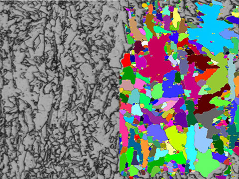
- Grain sizes
- Pores and other sub-µm structures
The combination of FIB and SEM adds the following capabilities to our repertoire:
- Generation of near-surface cross sections (view example video)
- Characterization of thin films and layer systems
- Preparation of STEM and APT samples
- 3D representation and calculation of microstructures
Additional built-in systems allow us to perform a holistic assessment:
- Chemical analysis of particles, layers or element distributions (EDX)
- Analysis of crystal orientations, grain size distributions, dislocation densities, textures, deformations and preferred directions (EBSD)
- Reconstruction of former austenite grains from EBSD data
- Investigation and chemical analysis of precipitates, phases and layers down to the sub-nm range (STEM incl. STEM-EDX)
- Locally resolved repairs, production of precise mask geometries and special mechanical components, targeted deposition of conductive and non-conductive compounds (micromachining) (view example video)

Hydrogen Embrittlement

STEM-Analysis

Layer Thickness Analysis

APT-Analysis
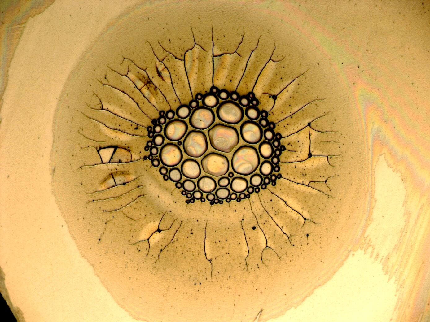
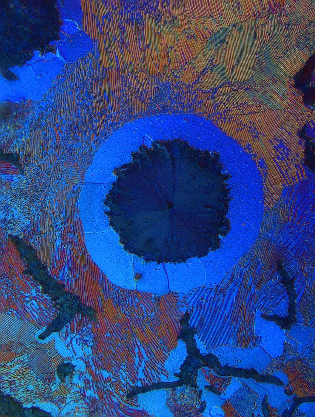
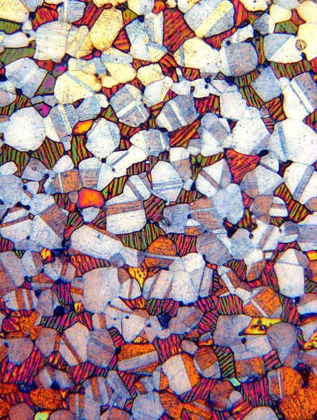
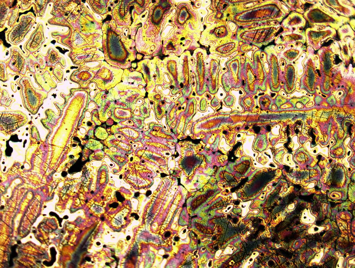
Microscopy examples


Further examinations

Surface analysis
In addition to the representation and analysis of surfaces, we also offer profile recordings to determine the layer system. We are not only at your side with the surface characterization, but can also change properties in a targeted manner.

Material analysis
Thanks to our spark spectrometer, we can determine the chemical composition of materials down to the ppm range. Other investigation methods in our portfolio are, for example, microstructure analyzes using FIB-REM technology, X-ray diffraction analyzes or 3D tomography.
Contact for questions
Dr.-Ing Dominik Britz
Deputy Head MECS Saarbrücken

Adrian Thome, M. Sc
Project Leader